Inside the CPU: how fetch, decode, execute turns electricity into software
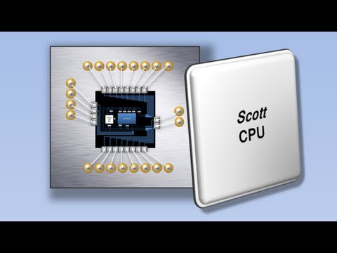 Photo: N43 and Hermes
Every app, every render, every answer runs on a three-beat loop older than the microprocessor itself. N43 follows the cycle from sand to 25-billion-transistor silicon, and asks what the oldest algorithm in computing is worth in the AI era.
Source video: How a CPU Works · In One Lesson · approximately 8.5 million views observed via yt-dlp on 2026-09-05. Independently researched by N43 and Hermes.
01 THE LOOP THAT RUNS THE WORLD
Every piece of software you have ever used - a spreadsheet, a video call, a language model - is ultimately a list of simple instructions, and the processor's entire job is to work through that list. It does so with a three-beat rhythm so old it predates the microprocessor itself: fetch the next instruction from memory, decode what it means, execute it. Nothing fundamental about that loop has changed since the first stored-program computers of the late 1940s.
The mechanics are disarmingly simple. A register called the program counter holds the memory address of the next instruction. Fetch pulls the instruction bytes at that address into the CPU. Decode circuitry works out what operation is being asked for and which data it applies to. Execute then carries it out - adding two numbers, loading a value, deciding whether to jump somewhere else - and the program counter moves on. Repeat a few billion times per second and you have modern computing.
Almost every clever trick inside a modern chip exists for one reason: to keep this loop fed. Pipelines let a new instruction start every cycle. Caches keep likely instructions close by. Branch predictors guess which way a decision will go before it is made. Understanding the loop is therefore not nostalgia - it is the key that explains the rest of the machine.
02 FROM SAND TO SWITCHES
Underneath the loop sits a device of almost unbelievable simplicity: the transistor, an electrically controlled switch with no moving parts. Carve billions of them out of purified silicon, wire them into logic gates, connect gates into adders, registers, and control units, and you have a processor. A modern desktop chip packs tens of billions of these switches into something smaller than a postage stamp.
The scaling that made this possible is one of the most reliable trends in industrial history. Intel's 4004, the first commercial microprocessor in 1971, used about 2,300 transistors. Apple's M3, released in 2023, uses roughly 25 billion - a growth factor of about ten million in barely fifty years, and the raw material behind every jump in computing capability since the 1970s.
CPU transistor counts, 1971-2023, as publicly reported (Wikipedia: Transistor count). Bar heights use a log-style scale; values are labeled explicitly on each bar. Publicly reported figures, not estimates.
03 THE CLOCK THAT SETS THE PACE
The loop needs a metronome. A crystal oscillator drives a clock that ticks billions of times per second - a 3.5 GHz chip has 3.5 billion opportunities each second to start a new instruction. For decades clock speed was the headline number in computing, doubling through the 1980s and 1990s and fueling the megahertz wars of the Pentium era.
The race hit a wall in the mid-2000s, and the reason is physics rather than marketing. The power a chip dissipates rises roughly with frequency and with the square of its voltage, and every watt must leave the die as heat. Around 2004-2005, single-core chips approaching 4 GHz became uncoolable at sane power budgets, and the industry abandoned the frequency race almost overnight.
Today the number that matters just as much is IPC - instructions completed per cycle - along with boost clocks that let a core sprint briefly inside a fixed thermal budget. A modern CPU is less a runaway engine than a carefully rationed one.
04 MORE CORES, NEW MATH
Stalled clocks left one obvious escape: if one core cannot go faster, add another. A core is a complete, independent engine capable of the full fetch-decode-execute cycle, and mainstream chips now carry from four to dozens of them - often mixed, with fast performance cores for demanding threads and small efficiency cores for background work.
Parallelism has its own arithmetic. Amdahl's law says the serial fraction of a program sets a hard ceiling on how much extra cores can help: if 20 percent of your code cannot be parallelized, ten thousand cores will never make it more than five times faster. Software has to be written to share the work, which is why core counts translate into real-world gains so unevenly.
The practical map: video encoding, compiling, simulation, and serving many users at once scale well with cores, while single-threaded tasks - much everyday application logic - barely notice the extras at all.
05 SHRINKING THE NODE
The engine behind both transistor counts and power efficiency is the manufacturing process - the lithographic recipe used to print the chip. Its name is the node: about 10,000 nanometers in 1971, 250 nm in 1996, 5 nm and 3 nm in the 2020s.
For decades the node name tracked a real physical feature, the length of the transistor gate. Since roughly the 22 nm generation it has been, candidly, a marketing label - a 5 nm process does not contain gates 5 nanometers long. What remains real is what shrinking delivers: more transistors per square millimeter, lower power per switch, and more performance in the same die area.
The cost side is brutal. A leading-edge fab now costs upward of 20 billion dollars, and only three companies - TSMC, Samsung, and Intel - operate anywhere near the leading edge. Shrinking continues, but the club that can do it keeps getting smaller.
CPU manufacturing process node shrink by era. Node names are marketing designations per era, not literal gate lengths. Log-style bar heights; values labeled explicitly. Illustrative timeline.
06 THE CPU IN THE AI ERA
The AI boom runs on accelerators - GPUs and dedicated matrix engines that crush the multiply-accumulate work at the heart of neural networks. It is tempting to read that as the CPU becoming irrelevant. The opposite is closer to true: every accelerator is a guest inside a system the CPU runs.
Watch what happens around a single large-model inference request. The CPU tokenizes the input, schedules batches, moves data between network cards, DRAM, and accelerator memory, and post-processes the output. Remove a capable host processor and the fastest GPU idles. Data center operators buy CPUs and accelerators as a matched pair for exactly this reason.
CPUs have also absorbed AI work directly: wide vector units such as AVX-512 on x86 and SVE on Arm, matrix extensions like AMX, and NPUs shipping in mainstream laptop and phone chips handle modest models locally. The boundary keeps moving, but it moves on top of the same old loop.
07 LIMITS, LEGACY, AND WHAT COMES NEXT
The honest limits: Dennard scaling - the rule that let smaller transistors also run at lower power - ended around 2006, leaving chips with dark silicon they cannot all switch at once. Gates are now counted in atoms, and each further shrink yields less at exploding cost. Nobody expects 50 GHz commodity chips anymore.
Yet the legacy is astonishing. The fetch-decode-execute cycle has survived vacuum tubes, magnetic cores, integrated circuits, and three-dimensional chip stacking without changing its shape. It is one of the most durable abstractions engineers have ever produced - instruction sets designed in the 1970s and 1980s still run unmodified on today's silicon.
What comes next is more specialization rather than replacement: chiplets assembled like building blocks, accelerators for every workload class, memory moved closer to compute. Each generation redraws the details. Underneath, the same three beats - fetch, decode, execute - will keep time for a long while yet.
By N43 and Hermes for Sailor Bob News.


