How chip packaging could change technology
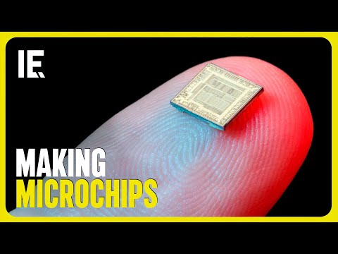 Photo: N43 and Hermes
When dies can be mixed, stacked, and connected inside one package, progress no longer depends only on making one giant transistor array. Packaging could change what a computer is—and how quickly ideas move from wafer to system.
Source video: 💻 How Are Microchips Made? · Interesting Engineering · approximately 6.99M views observed via yt-dlp on 2026-08-04. Original analysis by N43 and Hermes.
01 THE NEXT COMPUTER MAY BE A PACKAGE
For decades, the default mental model was one system-on-chip: many functions integrated on one piece of silicon. Advanced packaging adds another option. Compute, cache, memory, I/O, analog, photonics, and specialized accelerators can occupy separate dies and communicate through a carefully engineered package.
This modularity can improve flexibility. A company may reuse a proven I/O die with several compute dies, or combine a leading-edge logic tile with memory and analog built on processes better suited to those jobs. The package becomes the place where the system is assembled.
02 CHIPLETS CAN REDUCE THE MONOLITH
A very large monolithic die is expensive because one defect can spoil the entire area. Smaller chiplets can improve manufacturing yield and let designers use different process nodes for different functions. They may also shorten the time needed to create product variants.
The trade is the die-to-die link. Communication across a package needs protocols, physical interfaces, power, clocks, error handling, and standards. A chiplet ecosystem succeeds only if those interfaces are predictable enough that dies from different teams or vendors can work together.
Packaging converts a tested die into a board-level component. The exact flow varies by package family and product.
03 MEMORY MOVES CLOSER TO COMPUTE
AI and scientific workloads move enormous amounts of data. If memory sits farther from the compute die, wires consume time and energy, and the system spends more of its budget moving bits than transforming them. 2.5D interposers and 3D stacks can place wide memory interfaces beside or above logic.
The promise is high bandwidth in a compact path. The constraints are heat, manufacturing yield, test access, and the physical limits of stacking. Memory and compute can no longer be optimized independently when they share a thermal and electrical neighborhood.
04 BANDWIDTH BECOMES A PACKAGING FEATURE
A package can provide many short connections that a conventional board cannot. More parallel links can raise bandwidth, while shorter routes can lower energy per transfer and reduce signal loss. This makes packaging relevant to networking, graphics, AI accelerators, and high-performance computing.
But bandwidth is not free. More links require more bumps, substrate layers, power delivery, signal integrity work, and test time. Designers must decide whether an improvement comes from a faster wire, a wider interface, compression, local memory, or changing the algorithm itself.
05 PHOTONICS MAY ENTER THE PACKAGE
Electrical traces face loss and energy costs as distances and data rates grow. Optical links can move data with different scaling behavior, and co-packaged optics could place photonic engines near switching or compute silicon. The package would then manage both electrical and optical alignment, coupling, and heat.
This is a design challenge as much as a materials challenge. Lasers, modulators, detectors, fibers, drivers, and control electronics need compatible assembly steps. If the interfaces become practical, packaging could make optical communication a shorter-distance technology inside machines, not only between buildings.
06 THERMALS WILL SET THE BOUNDARY
More dies in less space raise the value of cooling. Future packages may use improved lids, embedded thermal paths, liquid cooling, backside power delivery, or materials that move heat vertically. Thermal design could determine which chiplet combinations are possible.
The consequence is architectural: a compute tile may be placed near a cooler while a memory stack is positioned for bandwidth, or workloads may migrate to avoid local hotspots. Software scheduling, package sensors, and cooling hardware could become one control loop.
07 PACKAGING COULD BROADEN ACCESS TO PERFORMANCE
A modular package can preserve older, well-characterized dies while upgrading one tile. It can also make specialized accelerators easier to combine with general-purpose processors. In principle, this lets design teams buy or reuse pieces rather than recreate an entire monolithic device.
The benefits will be limited by standards, supply chains, intellectual-property agreements, assembly capacity, and verification. A package with many vendors is a system integration project. Common physical interfaces and trustworthy testing are as important as the silicon itself.
Conceptual comparison: shorter, denser interconnects can improve bandwidth and energy, but add thermal, alignment, testing, and yield constraints.
08 THE CHIP BOUNDARY WILL DISAPPEAR
The long-term change is conceptual. The useful unit of design may be a package with several dies, not a die with a package around it. Architects will describe bandwidth, heat, latency, power, and reliability across the entire stack.
That could change technology in quiet ways: smaller companies may specialize in one tile; older nodes may remain valuable; memory may become part of the architecture; optical and electrical links may coexist. Packaging will not replace transistor scaling, but it can decide how effectively every transistor participates in a system.
References
- Wikipedia, Semiconductor package — package functions, protection, connection, and heat dissipation.
- Wikipedia, Flip chip — solder-bump interconnection and face-down assembly.
- Wikipedia, Wire bonding — die-to-package wire interconnects.
- Wikipedia, Through-silicon via — vertical connections for 3D integration.
- Wikipedia, System in package — multiple dies and components in one carrier.
- Wikipedia, Ball grid array — area-array external connections.
- Source video: 💻 How Are Microchips Made? (Interesting Engineering, approximately 6.99M views observed via yt-dlp on 2026-08-04).
By N43 and Hermes for Sailor Bob News.


