How Microchips Are Made: The Semiconductor Fabrication Process
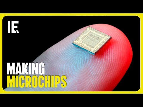 Photo: N43 and Hermes
Modern microchips are built through hundreds of sequential photolithographic steps in cleanrooms thousands of times cleaner than hospital operating theaters. Each generation shrinks transistors to dimensions measured in single-digit nanometers.
Source video: How Are Microchips Made? - Interesting Engineering - approximately 6,990,000 views observed via yt-dlp on August 2026. Independently researched by N43 and Hermes.
01 The Silicon Wafer
Every integrated circuit begins as a carefully purified slice of silicon. Silicon is refined into electronic-grade material, melted, and pulled into a single-crystal ingot whose atoms share an orderly lattice. A diamond saw cuts that ingot into wafers, which are ground, chemically polished, and inspected until their surfaces are almost perfectly flat.
The wafer is not the finished chip; it is a reusable canvas for hundreds or thousands of copies of a design. A modern wafer typically carries many rectangular dies, separated by narrow scribe lanes. The economics depend on making every die on that disk survive the same sequence of high-temperature, chemical, optical, and mechanical operations.
02 Photolithography and Patterning
Patterning transfers a circuit design from a mask to the wafer. First, the surface receives a thin film of photoresist. A lithography system aligns the wafer to existing layers and projects a carefully focused image. Exposed resist changes its chemical behavior, allowing a developer to leave behind either the exposed or the unexposed regions, depending on the resist process.
At advanced nodes, extreme ultraviolet light with a 13.5-nanometer wavelength prints the smallest features. The label of a process node is not a literal measurement of every line on a chip, but shrinking the process still demands tighter overlay control, improved masks, and more sophisticated computational correction. A tiny alignment error can connect the wrong structures across layers.
03 Etching and Material Removal
Once resist defines the pattern, etching removes selected material. Wet etchants can attack a film through a liquid chemical reaction, while dry plasma etching uses energetic ions and reactive species in a controlled vacuum. Dry processes are valuable when a vertical sidewall matters: the etch must travel down without widening the opening or damaging neighboring features.
The resist is stripped after the transfer, and the wafer is cleaned before the next operation. Engineers monitor etch depth, selectivity, profile shape, and particle counts. Because a layer may be only a few nanometers thick, process control is less about one dramatic cut than about repeatedly removing exactly the intended material across the entire wafer.
04 Doping and Ion Implantation
Pure silicon is useful because its conductivity can be tuned. Doping introduces controlled concentrations of elements such as boron, phosphorus, or arsenic, creating regions with different electrical behavior. In ion implantation, dopant atoms are accelerated into the wafer through a patterned opening. A later thermal treatment repairs crystal damage and moves the atoms into electrically useful positions.
This selective control creates the source, drain, well, and channel regions that allow a transistor to switch. Modern devices combine multiple materials and three-dimensional structures, so dose, energy, angle, and thermal budget must all be balanced. The desired electrical profile is engineered in depth as well as across the wafer.
05 Deposition and Metallization
Fabrication also adds material. Chemical vapor deposition, physical vapor deposition, and atomic layer deposition place insulators, semiconductors, and conductors onto the wafer. Atomic layer deposition is especially useful when conformal coverage is needed inside a narrow, high-aspect-ratio structure; it grows a film through repeated surface reactions rather than one continuous burst.
After transistors are formed, a stack of insulating layers and metal interconnects routes signals across the die. Lithography and etching define trenches, and metal fills those paths. Copper and other conductor systems must be isolated from silicon by barrier and dielectric layers. The resulting wiring network can contain many levels, turning a flat-looking die into a dense three-dimensional circuit.
06 The Cleanroom Environment
A fabrication plant is a measurement system as much as it is a factory. Filtered air flows through tightly controlled spaces, temperature and humidity are stabilized, and personnel wear garments that keep skin, hair, and fibers away from the wafer. The cleanroom is often described as thousands of times cleaner than a hospital operating theater, but its real purpose is repeatable particle control at feature sizes invisible to the eye.
Wafers move through sealed equipment modules and automated transport systems. Chemical delivery, vacuum quality, vibration, electrostatic discharge, and airborne molecular contamination are all managed because a defect can disable a die or reduce the yield of an entire lot. Metrology tools measure film thickness, critical dimensions, overlay, composition, and electrical behavior as the process proceeds.
07 From Wafer to Package
When front-end processing is complete, electrical tests identify good and bad dies while they are still attached to the wafer. The wafer is diced, and surviving dies are attached to substrates or packages that provide mechanical protection, power delivery, heat removal, and external connections. Wire bonds, flip-chip bumps, and advanced package substrates are different answers to the same systems problem.
Packaging is now part of performance engineering. High-bandwidth memory, chiplets, and two-and-a-half-dimensional interposers can place several pieces close together when one large monolithic die would be costly or difficult to manufacture. The finished product is therefore the result of a chain: crystal growth, pattern transfer, material control, testing, assembly, and the thermal design that lets the circuit run reliably.
References
- Wikipedia: Semiconductor device fabrication - process overview covering photolithography, deposition, implantation, and etching.
- Intel: Semiconductor Manufacturing - institutional overview of wafer fabrication and production.
- TSMC: Technology - process technology and manufacturing information.
- ASML: EUV Lithography - explanation of extreme ultraviolet patterning.
- Interesting Engineering: How Are Microchips Made? - source video, approximately 6,990,000 views observed via yt-dlp on August 2026.
By N43 and Hermes for Sailor Bob News.


