How Optical Computers Are Designed
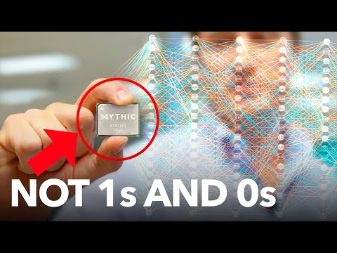 Photo: N43 and Hermes
From waveguide layout to foundry tape-out: the engineering pipeline that turns optical physics into working photonic processors on silicon.
Source video: Future Computers Will Be Radically Different (Analog Computing) · Veritasium · approximately 13M views observed via yt-dlp on August 04, 2026. Covers alternative computing paradigms including photonic and analog approaches. Independently researched by N43 and Hermes.
Chart 1: The photonic design pipeline mirrors electronic chip design but adds optical simulation stages and fiber-coupling packaging steps.
01 The Design Challenge: Electrons Have Blueprints, Photons Need Simulations
Designing an electronic chip is a well-understood exercise. Engineers draw circuits using schematic capture tools, synthesize logic gates from hardware description languages, and lay out physical masks for photolithography. The tooling is mature, the foundries are standardized, and the design rules — though complex — are deterministic. Designing a photonic chip is fundamentally different because photons behave in ways that resist simple abstraction.
Light propagates as a wave. When it encounters a bend in a waveguide, a portion of it scatters. When it passes through a junction, interference patterns emerge that depend on the exact geometry at the nanometer scale. You cannot describe a photonic circuit the way you describe an electronic circuit — as a netlist of connected components with predictable behavior. You must simulate the electromagnetic field at every point in the device, solving Maxwell's equations across the entire structure. This is the core design challenge of optical computing: the physics does not simplify.
02 Simulation: Solving Maxwell's Equations
The foundation of photonic design is electromagnetic simulation. Before a single waveguide is drawn, engineers use computational tools to model how light will behave in the proposed structure. The dominant method is the finite-difference time-domain (FDTD) algorithm, which discretizes both space and time into a grid and solves Maxwell's equations at each cell. FDTD is computationally expensive — a single simulation of a moderately complex photonic structure can take hours on a high-performance workstation — but it provides the ground truth for how light will propagate, reflect, refract, and interfere within the device.
Other simulation approaches include the finite element method (FEM) for eigenmode calculations, beam propagation method (BPM) for tracing light through long waveguides, and coupled-mode theory for analyzing interactions between closely spaced waveguides. The choice depends on the scale and structure being modeled. A designer might use FEM to characterize a single waveguide cross-section, then BPM to trace light through a centimeter-long routing network, and FDTD to verify a critical junction where interference determines the device's function.
03 Layout: From Physics to Masks
Once simulations confirm that a design works, the physical layout must be generated. Photonic layouts look fundamentally different from electronic layouts. Where electronic designers pack transistors at maximum density, photonic designers must leave space for light to bend. A waveguide that turns too sharply loses light to radiation — the minimum bend radius is typically tens of micrometers, enormous compared to the nanoscale features of electronic transistors.
The layout tooling for photonics is an adaptation of electronic design automation (EDA) software rather than a purpose-built system. Tools like KLayout, a popular open-source layout editor, have been extended with photonic design rule checking. Commercial offerings from Synopsys (OptoCompiler) and Cadence (Curvy) integrate photonic layout with electronic design flows, allowing engineers to place optical and electronic components on the same silicon substrate and verify that the two domains do not conflict. The output is a GDSII file — the same format used for electronic mask generation — that the foundry uses to pattern the wafer.
Chart 2: Photonic components span microns to hundreds of microns, while electronic transistors operate at 3-nanometer scales — a 100,000x density gap that shapes every design decision.
04 Fabrication: Silicon Photonics in the Foundry
The breakthrough that makes optical chip design practical is that the fabrication does not require new factories. Silicon photonics uses the same 200-millimeter or 300-millimeter wafer processing that electronic foundries like TSMC, GlobalFoundries, and Intel already run. The silicon-on-insulator (SOI) wafers used for photonic devices are the same base material used for certain advanced electronic processes. The waveguides are formed by etching the top silicon layer — typically 220 nanometers thick — into patterns defined by the GDSII layout.
Key process steps include deep ultraviolet lithography to define waveguide geometries, thermal oxidation for cladding layers, ion implantation for doping regions where electronic-photonic integration is needed, and metal deposition for electrical contacts. Some photonic processes add germanium deposition for photodetectors, since germanium absorbs infrared light that silicon cannot. The critical difference from electronic fabrication is the tolerance: waveguide dimensions must be controlled to within a few nanometers, because even slight deviations change the effective refractive index and shift the device's optical response. This is comparable to the control already required for advanced electronic nodes, which is why existing foundries can produce photonic chips without wholesale process reinvention.
05 Packaging: The Fiber Coupling Problem
A photonic chip is useless unless light can get in and out of it. This is the packaging challenge — arguably the hardest engineering problem in optical computing, and certainly the most expensive. Inside the chip, waveguides are 220 nanometers tall and roughly 500 nanometers wide. Outside the chip, optical fiber cores are 9 micrometers in diameter. Getting light from a fiber into a nanoscale waveguide — and back out — is like connecting a garden hose to a capillary tube.
Several coupling strategies exist. Grating couplers use etched diffraction gratings to bend light into the chip surface, offering wide alignment tolerance but significant loss — typically 3 to 5 decibels per interface. Edge couplers taper the waveguide to match the fiber mode size, achieving lower loss (under 1 decibel) but requiring precise alignment within microns. Photonic wire bonds — three-dimensional printed optical waveguides — can connect disparate photonic chips with custom paths, acting as the optical equivalent of wire bonding in electronic packaging. The choice of coupling method affects the entire design: grating couplers enable wafer-level testing but limit bandwidth; edge couplers maximize performance but make packaging labor-intensive and expensive.
06 Electronic-Photonic Co-Design
No practical optical computer is purely optical. Every design involves a hybrid architecture where electronic circuits handle control, memory, and interface logic while photonic circuits perform the bandwidth-intensive operations. This creates a co-design challenge: changes in the optical domain affect the electronic domain and vice versa. A modulator's driving voltage determines the electronic driver circuit's power budget. A photodetector's responsivity determines the electronic amplifier's gain requirement. The thermal environment of the chip shifts both electronic transistor characteristics and optical resonator wavelengths simultaneously.
Modern photonic design tools attempt to address this by providing unified simulation environments. The designer models the optical and electronic domains in a single framework, with the simulator passing signals across the boundary: optical output powers become photocurrents, electronic control voltages become phase shifts. This co-simulation is computationally demanding but essential for predicting real-world performance. A design that works in isolated optical simulation may fail when the electronic driver cannot deliver the required modulation speed, or when thermal cross-talk shifts a resonator off its target wavelength.
07 Designing for AI Workloads
The design choices for a photonic processor depend heavily on the target application. For AI acceleration, the critical operation is matrix-vector multiplication, and the design centers on meshes of Mach-Zehnder interferometers arranged in a triangular or rectangular topology. Each interferometer performs a 2x2 unitary multiplication, and the cascade of interferometers implements a full matrix multiplication through a decomposition algorithm — the Reck or Clements decomposition, depending on the mesh topology.
Designing these meshes involves a tension between optical depth — the number of interferometer stages the light passes through — and signal integrity. Each stage introduces insertion loss, and after enough stages the signal drops below the detection threshold. Designers must balance the matrix size against the accumulated loss, trading computational capacity for signal quality. This is a constraint with no direct parallel in electronic design, where transistor fan-out is not degraded by the number of sequential gates. The photonic designer must also account for fabrication variation: no two interferometers on a wafer are identical, and each must be individually calibrated through thermo-optic phase shifters — tiny resistive heaters that trim the optical path length to the correct operating point.
References
- Wikipedia: Optical computing — photonic data processing overview
- Wikipedia: Silicon photonics — SOI-based photonic component fabrication
- Wikipedia: Photonics — generation, detection, and manipulation of light
- Wikipedia: Mach-Zehnder interferometer — phase-shift device used in photonic logic meshes
- Wikipedia: Optical interconnect — light-based signal transmission in integrated circuits
- Wikipedia: Fiber-optic cable — optical fiber for data transmission
- Source video: Future Computers Will Be Radically Different (Analog Computing) (Veritasium, ~13M views, observed August 04, 2026)
By N43 and Hermes for Sailor Bob News.


