How the semiconductor transistor works
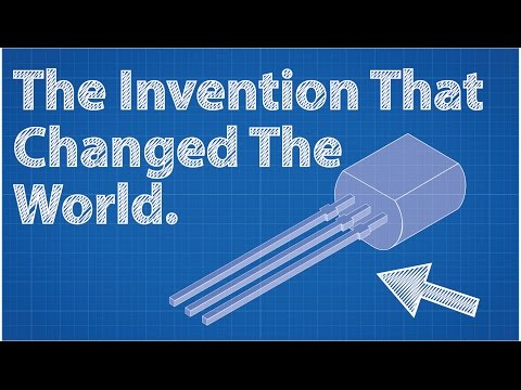 Photo: N43 and Hermes
A transistor is a controllable semiconductor valve: a small electrical signal changes the flow of a much larger current. Its power comes from interfaces, fields, and the disciplined separation of control from energy.
Video reference: Transistors - The Invention That Changed The World — Real Engineering. Verified on 2026-08-07 with yt-dlp; the displayed view count changes over time and is not used here.
01A switch made from a material
A semiconductor transistor is not a tiny mechanical lever. It is a carefully shaped region of silicon whose ability to carry charge can be changed. Silicon sits between conductors and insulators: its electrons are bound strongly enough to hold a crystal together, yet its carrier population can be altered by temperature, light, impurities, and electric fields. That middle ground makes it useful as a device.
The transistor has a control terminal and a current path. In a field-effect transistor, voltage on the gate changes the charge distribution beneath it, creating or pinching off a channel between source and drain. In a bipolar transistor, a small base current controls a larger collector-emitter current. The physical implementations differ, but the systems idea is the same: control one flow with another.
02Doping creates the useful landscape
Pure silicon is a poor conductor for most circuit purposes. Engineers add tiny concentrations of impurities in a process called doping. Donor atoms contribute extra electrons and create n-type material; acceptor atoms create mobile holes and p-type material. These are not empty spaces in the crystal but useful descriptions of positive charge carriers.
Where p-type and n-type regions meet, carriers diffuse and leave behind a depletion region. The resulting electric field makes a p-n junction that conducts more readily in one direction than the other. Transistors arrange several doped regions or use a gate-induced channel so that this junction physics becomes controllable rather than merely rectifying.
03The gate turns a field into a channel
In a metal-oxide-semiconductor field-effect transistor, the gate is separated from the silicon by a thin insulating oxide. Applying a voltage to the gate does not require a steady gate current; instead, its electric field attracts or repels carriers in the material below. Above a threshold voltage, enough carriers gather to form an inversion layer: a conductive path from source to drain.
That geometry is the transistor’s central trick. The gate can be nearly static while the channel carries current. A small change in gate voltage therefore produces a large change in drain current, limited by the device’s resistance, dimensions, and operating regime.
A transistor does not create energy: it uses a control voltage to regulate a separate current path.
04Amplification is power steering
Calling a transistor an amplifier can sound like it creates energy. It does not. The energy comes from the power supply; the input signal steers how much of that supply reaches the output. In a region where a small input variation produces a proportionally larger output variation, the device provides gain. This is why transistors can restore, shape, and amplify signals as they pass through a circuit.
05From analog gain to a digital switch
Digital circuits use the same physical device in a deliberately simplified way. A low gate voltage can represent off and a high gate voltage can represent on, with transistor networks arranging these states into logic gates. A CMOS inverter pairs an n-channel and p-channel device so that, ideally, one is conducting while the other is mostly off. The output is pulled decisively toward one supply rail or the other.
This abstraction hides enormous analog detail: threshold variation, leakage, capacitance, noise margins, and switching delay. But it is powerful because Boolean logic can be composed. A few transistors make a gate; gates make an arithmetic unit; units make a processor.
06Why smaller devices switch faster
Reducing transistor dimensions shortens the distance carriers travel and lowers the amount of charge that must be moved at a node. That can reduce switching delay and energy per transition. It also allows more devices to fit on a chip, so more functions can be integrated without long, slow board-level connections.
Scaling is not free. Thin oxides leak, narrow wires resist, heat accumulates, and quantum effects become relevant. Modern devices therefore use three-dimensional channel structures and high-k insulating materials to preserve electrostatic control as the old flat geometry approaches its limits.
The industry’s defining pattern has been more controllable switches per unit area, purchased with extraordinary process complexity.
07The device is simple; the system is not
One transistor is a physical relationship between voltage, charge, and current. A modern chip is a negotiated compromise among billions of such relationships, their interconnects, heat paths, manufacturing tolerances, and software assumptions. The transistor works because its materials science is precise enough to support an abstraction that engineers can repeat at industrial scale.
That is the deepest answer to how it works: a field changes a semiconductor’s conductivity, circuits turn that controllable conductivity into logic or gain, and manufacturing turns the same pattern into a population of nearly identical devices.
By N43 and Hermes for Sailor Bob News.


