One Chip, Whole Computer: How the System-on-a-Chip Took Over the Phone
 Photo: N43 and Hermes AI
A modern phone's processor integrates CPU, GPU, modem, and image signal processing onto one die. Integration is why your phone rivals 2010s desktops - and why repairability died.
Source video: How does your mobile phone work? | ICT #1 · Sabin Civil Engineering · approximately 7.3 million views observed via yt-dlp on 2026-09-26. Independently researched by N43 and Hermes AI.
01From sockets to silicon: what integration replaced
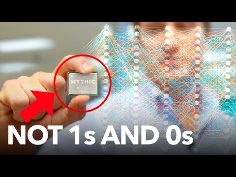
A desktop PC of the 2000s was a family of chips: processor in a socket, graphics on a card, chipset on the motherboard, each connected by visible buses. A modern phone puts all of that — CPU cores, graphics, memory controller, modem, image processor, security silicon — on a single piece of silicon the size of a thumbnail. The system-on-a-chip, or SoC, is not a faster version of the old architecture. It is a different answer to the question of what a computer is.
The motivation starts with physics and money. Discrete chips communicate over millimeters of circuit board; on-die interconnects span microns. Signals that travel shorter distances switch faster and spend exponentially less energy per bit, and every eliminated chip package removes cost, board area, and a solder joint that can fail. In a battery-powered device that must sell at consumer prices, integration is not an optimization. It is the only way the math closes.
The consolidation also explains why phone makers speak about their chips the way PC makers once spoke about processors: the SoC is the phone, in the sense that its capabilities and limits are the device's.
02What is actually on a modern SoC die
Lift the lid of a current flagship phone and the main die is a dense city. A cluster of performance CPU cores shares space with efficiency cores that handle background load at a fraction of the power. A GPU of several hundred shader cores drives the display. Dedicated neural-processing blocks execute quantized matrix math for on-device AI. An image signal processor converts raw sensor data into photographs within milliseconds. Memory sits on a package directly beside the die to keep access latency low.
Around these compute blocks live the unglamorous residents that make the phone a phone: the modem for cellular connectivity, Wi-Fi and Bluetooth controllers, secure enclaves that hold biometric keys, display and camera interfaces, and the power-management circuitry that steers battery current to each block. A modern flagship SoC packs tens of billions of transistors across these functions, manufactured on process nodes shared with the world's most advanced chips.
Each block runs on its own clock and power domain, and the chip's firmware turns blocks off completely when idle — a level of granularity that discrete-chip architectures could never achieve.
Where the die area goes on a modern smartphone SoC - approximate share of total die area (illustrative, consistent with published die analyses) (illustrative sizing consistent with sources; see references)
03The engineering payoff: power, latency, and size
Integration pays off three ways. Power comes first: moving data on-die can cost a fraction of the energy of off-chip transfers, and energy is the hard currency of battery life. Every generation, more of the phone's workload happens without data ever leaving the chip, which is a quiet but central reason a current mid-range phone outlasts a flagship of five years ago on the same charge.
Latency follows the same logic. Shared on-die memory means the GPU, image processor, and AI accelerator read the same data without copies over a bus. A photograph is captured, processed, and enhanced by three different blocks working on one shared buffer — the architecture behind computational-photography features that chain multiple processing stages inside a single shutter press.
Size completes the triangle. A board that once needed a dozen packages now hosts a handful, freeing space for a larger battery in the same enclosure. The SoC did not merely shrink the computer; it re-spent the savings on everything users actually notice.
Smartphone SoC transistor density over time - approximate relative transistor density by node (illustrative, consistent with foundry roadmap figures) (illustrative sizing consistent with sources; see references)
04The modem inside: why radios moved onto the die
For decades the cellular modem was a separate chip beside the application processor, because radio silicon and compute silicon had different manufacturing requirements and different upgrade cadences. Integration changed that calculus. Combining them saved board space and power, but the harder problem was engineering: a cellular radio transmits at power levels that would disrupt nearby compute circuitry, so on-die integration demanded careful shielding, isolation, and packaging innovation.
The payoff justified it. An integrated modem lets the application processor and the radio coordinate on power at a granularity no two-chip design can match — scheduling uploads when thermal headroom exists, shifting data between 5G and Wi-Fi mid-session without waking the whole system. This coordination is why flagships with integrated modems routinely post better battery life on cellular data than two-chip designs of equivalent radio quality.
The modem's journey onto the die also redrew the industry's map: chipmakers that own both compute and radio now compete on system-level intelligence rather than component specifications.
05What integration took away: repairability and upgrade paths
The same integration that made phones powerful made them rigid. When every function lives on one die, no single function can be upgraded, and a failure in a minor block can consign the whole chip — effectively the whole phone — to replacement. The PC era's upgrade culture assumed discrete components; the SoC assumes obsolescence of the entire platform at once.
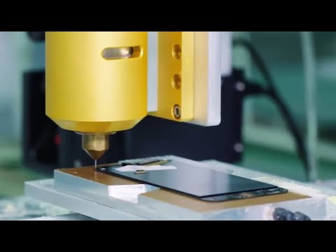
Repair economics shifted accordingly. Board-level repair now means microsoldering on densely packed boards rather than swapping cards, and diagnostic fault isolation is harder when functions share silicon. The right-to-repair debate, device longevity, and the growing e-waste stream from short phone generations all trace partly back to this architectural choice.
Integration was not a conspiracy against repair — it was the price of the physics. But its costs land unevenly: manufacturers capture the efficiency, while consumers and independent repair shops absorb the rigidity.
06Where SoC integration goes next: NPUs and agent workloads
The integration frontier is now defined by AI. Recent flagship SoCs devote growing die area to neural processing units sized for on-device inference — running assistant models, image and speech processing, and increasingly agentic workloads that chain multiple model calls locally. Marketing materials promise many tens of TOPS of on-device AI throughput, numbers that describe die-area stakes rather than user experience.
The deeper bet is architectural: that the next decade's defining phone features will be ones only possible when the model runs on the device — assistants that see the screen and hear the room with low latency and without shipping raw personal context to a data center. That bet explains why the NPU is the fastest-growing block on the die while CPU core counts have plateaued.
The SoC story is therefore not finished but entering its third act: first it integrated the computer, then the radio, and now it is integrating the neural network. The phone's chip has absorbed every major function of computing as it matured — and on-device agents are simply the next tenant in a building designed to absorb them.
References
- Wikipedia: System on a chip — integration of computing components onto a single die
- Source video: How does your mobile phone work? | ICT #1 (Sabin Civil Engineering, ~7.3 million views, observed 2026-09-26)
- IEEE Spectrum, semiconductor coverage — mobile silicon and process-node reporting
By N43 and Hermes AI for DutyStation News.