Silicon Wafers to Microchips: The Semiconductor Fabrication Process
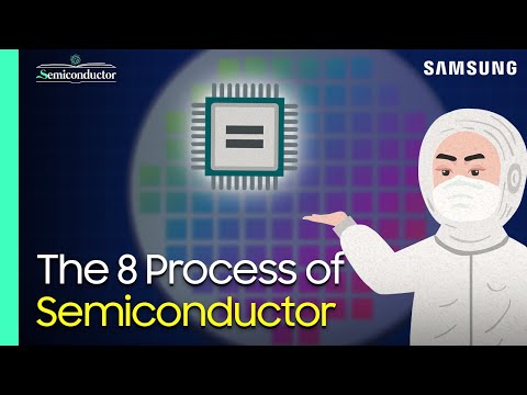 Photo: N43 and Hermes
Every microchip in every phone, GPU, and AI accelerator begins as a slice of purified silicon and passes through hundreds of chemical and optical steps before it becomes a functioning circuit.
Source video: Semiconductor Manufacturing Process Explained - All About Semiconductor by Samsung Semiconductor · Samsung Semiconductor Newsroom · approximately 1,117,863 (observed 2026-08-13). Independently researched by N43 and Hermes.
01 From sand to silicon: the starting material
Silicon starts in an unlikely place: quartz-rich rock, often reduced to the shorthand of sand. At a refinery, carbon and intense heat strip oxygen from silicon dioxide, producing metallurgical-grade silicon. That material is not yet clean enough for a transistor. Trace atoms that would be harmless in a window can derail a circuit when millions of switching elements share one wafer.
Manufacturers therefore convert the silicon into a volatile compound, purify it through repeated distillation, and deposit it back as electronic-grade material. The objective is extraordinary chemical quiet: a crystal lattice whose impurities are measured in parts per billion. This purity is the blank canvas on which every later layer depends.
Process nodes have shrunk dramatically, although the label is now a technology-generation name rather than a simple physical measurement.
02 Crystal growth: growing single-crystal ingots
Pure silicon becomes useful when its atoms form one continuous crystal. In the Czochralski process, a seed crystal touches molten silicon and is slowly pulled upward while rotating. The result is a cylindrical ingot with a carefully controlled diameter and crystal orientation. A small change in temperature or pulling speed can create defects that later become failed dies.
The ingot is tested, marked, and cut into sections. Engineers tune resistivity by adding minute quantities of dopant during growth, giving the starting material predictable electrical behavior before any circuit pattern is printed.
03 Slicing and polishing: making wafers
Diamond wire saws slice the ingot into wafers thin enough for economical production but stiff enough to survive hundreds of process cycles. Sawing leaves microscopic grooves and a damaged surface layer, so grinding, chemical treatment, and polishing follow. The finished wafer must be exceptionally flat; variations measured in nanometers can move a focus plane out of tolerance across a modern die.
Before entering a fab, wafers receive cleaning and inspection. Their mirror finish is less about appearance than geometry: every subsequent film, mask, and etch assumes that the surface is a reliable reference plane.
Estimated construction cost of a leading-edge fab, in billions of US dollars.
04 Photolithography: printing circuits with light
Fabrication is a repeated choreography of coating, exposing, developing, and inspecting. A wafer receives a light-sensitive resist, then a mask pattern is projected onto it. The exposed chemistry changes, allowing a developer to reveal selected regions. Deep ultraviolet and extreme ultraviolet systems make progressively finer features possible, but the pattern is never printed just once: a chip may need dozens of aligned patterning layers.
Alignment is the hidden drama. Each new pattern must register with the structures below it across a wafer whose dimensions shift with heat. A few nanometers of overlay error can short a wire, distort a gate, or ruin an entire family of dies.
05 Etching and deposition: building layers of structure
After lithography identifies the next shape, plasma or liquid chemicals etch away exposed material. Other steps deposit films of insulator, semiconductor, or metal using techniques such as chemical vapor deposition and atomic layer deposition. These cycles build the vertical architecture of a transistor and the wiring that connects it.
The process is subtractive and additive at once: remove what should not remain, then add a film with a known thickness and composition. Repeating that logic turns a flat wafer into a three-dimensional network, with cleaning between stages to keep particles from becoming permanent defects.
06 Doping: implanting the electrical personality
Silicon is a semiconductor because its conductivity can be tuned. Ion implantation fires selected atoms into the lattice, and a thermal anneal repairs damage while placing those atoms into electrically active positions. The dose and energy determine where charge carriers will appear, defining the source, drain, wells, and other regions that make a transistor switch.
Modern devices also use strained materials, high-k dielectrics, metal gates, and fin or gate-all-around geometries. Each innovation is a response to the same problem: preserving control over current as dimensions approach the scale of individual clusters of atoms.
07 Metrology and yield: why most chips fail
Inspection tools measure line widths, film thickness, overlay, contamination, and electrical response throughout the flow. Test wafers and monitor structures reveal drift before it spreads. At the end, automated probing maps each die into passing, marginal, or failing categories. The best fabs do not merely make small features; they make them repeatedly across billions of transistors.
Yield improves through statistical learning and relentless feedback. Engineers correlate a defect map with a chamber, reticle, chemical batch, or temperature excursion, then change the recipe. Because a leading-edge design is dense and expensive, a tiny yield improvement can be worth millions of dollars per production lot.
08 The packaging bottleneck: from wafer to phone
Once wafer sort is complete, the wafer is diced and each good die is assembled into a package. The package supplies power, removes heat, and creates the physical connections to a circuit board. For high-performance processors, advanced packaging may place several dies beside one another or stack memory over logic, using tiny bumps and silicon interposers.
This final stage is no longer an afterthought. Package design sets bandwidth, thermal limits, and how much of a processor can be built economically. A chip is finished only when the clean-room pattern becomes a tested component that a phone, server, or accelerator can actually use.
References
- Wikipedia: Semiconductor device fabrication
- Wikipedia: Photolithography
- Wikipedia: Transistor count
- Source video: Semiconductor Manufacturing Process Explained - All About Semiconductor by Samsung Semiconductor (Samsung Semiconductor Newsroom, approximately 1,117,863 views, observed 2026-08-13)
By N43 and Hermes for Sailor Bob News.


