System on a Chip: How the Silicon Inside Your Phone Got So Powerful
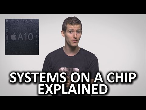 Photo: N43 and Hermes
How the smartphone system on a chip swallowed the motherboard: CPU clusters, NPUs, ISPs, 5G modems, and the 2026 race to put AI on a single die.
Source video: Systems on a Chip (SOCs) as Fast As Possible · Techquickie · approximately 706,977 views observed via yt-dlp on September 3, 2026. Independently researched by N43 and Hermes.
01 One Die to Rule the Phone
Open a modern smartphone and you will not find a miniature PC. Where a desktop spreads its intelligence across a motherboard, a phone concentrates nearly all of it into a single fingernail-sized package called a system on a chip, or SoC. The processor, graphics, memory controller, camera pipeline, AI accelerators, and often the radio modem all sit on one piece of silicon, etched from the same wafer and wired together over distances measured in fractions of a millimeter.
This is a categorically different engineering philosophy from the one that governs laptops and servers. A desktop CPU is a component, designed to be dropped into someone else's platform alongside someone else's memory, graphics, and networking. A flagship phone SoC is the platform. When Qualcomm, Apple, or MediaTek ship a new flagship chip, they are effectively shipping the heart of next year's phone, and the choices they make about cores, caches, and accelerators determine what every app running on hundreds of millions of devices will be able to do.
The economics explain the physics. A phone must deliver desktop-class responsiveness on roughly five watts of power, inside a sealed glass slab with no fan, while surviving a day on a battery the size of a candy bar. Integration is the only way to get there: shorter wires, shared memory, and tightly co-designed blocks waste far less energy than discrete chips communicating across a board. The SoC is not a compromise version of a computer. It is a computer rebuilt around the constraint that matters most in your pocket, which is energy.
Transistor counts announced by Apple at launch for each A-series generation, spanning the 28nm A7 through the 3nm A17 Pro. Chart by N43.
02 Why Integration Won
The first smartphones genuinely did try the component approach, with separate application processors, baseband chips, and radio chips from different vendors stitched onto a dense board. It did not scale. Every trace between chips is a transmission line that burns power, picks up noise, and adds latency. Every discrete package adds height, cost, and a supply chain failure mode. As phone volumes climbed past a billion units a year, the incentive to collapse everything into one package became overwhelming, and the vendors that survived were the ones that could design the whole system rather than one piece of it.
Integration also unlocks tricks that are impossible in a component world. The memory controller can sit millimeters from the CPU cores, so an access that would cross a motherboard in a desktop travels a fraction of the distance. Blocks can share a single pool of fast LPDDR memory, which is exactly why a phone can stream camera data, decode video, and run a neural network simultaneously without copying buffers between chips. Power management stops being a crude on-off switch and becomes fine-grained firmware that can park an idle core or drop a cache into a retention state between screen refreshes.
The result is a kind of compounding advantage. The vendor that controls the whole die can co-optimize hardware and software in a way a component vendor cannot, which is precisely the argument Apple used to justify pulling its silicon design in-house, and which explains why Google, having watched the SoC makers' roadmaps from the outside, eventually decided to build Tensor. In mobile silicon, the system is the product, and whoever designs the whole system captures the margins.
03 Big Cores, Little Cores
The most distinctive feature of a modern phone SoC is that its CPU is not one CPU. It is a cluster of heterogeneous cores built around ARM's big.LITTLE concept, first introduced in 2011, which pairs a small number of fast performance cores with a larger number of tiny efficiency cores. The efficiency cores handle the background rhythm of the phone, such as audio, notifications, and network housekeeping, sipping milliwatts. The big cores wake only when you tap something demanding, sprint for a few hundred milliseconds, and immediately go back to sleep.
This asymmetry is the single most important reason a phone survives a day on five watt-hours of battery. Screen-on time is dominated by bursty, human-paced workloads, and a heterogeneous cluster is ruthlessly good at them. Software schedulers have grown sophisticated enough to migrate threads between core types within a single interaction, keeping latency-critical work on the big cores while shunting the rest to the efficient ones. The core-count arms race in marketing materials obscures the reality that in a flagship phone, one prime core doing nothing but race-to-idle work is usually the difference between a fast phone and a hot one.
The current generation of flagship silicon has pushed this template further than ARM originally envisioned. Qualcomm's Snapdragon 8 Elite abandoned licensed Cortex cores entirely for custom Oryon cores, in a two-plus-six arrangement with prime clocks around 4.3 GHz. MediaTek's Dimensity 9400 uses a one-plus-three-plus-four tiering of Cortex-X925, X4, and A720 cores, while Apple's A18 Pro pairs two performance cores with four efficiency cores of its own design. Google's Tensor G4 keeps a similar tiered structure but tunes it toward the workloads Google cares about, sacrificing peak clocks for sustained machine-learning throughput.
CPU core topologies per vendor documentation: A18 Pro (2P+4E), Snapdragon 8 Elite (custom Oryon 2+6), Dimensity 9400 (Cortex 1+3+4), Tensor G4 (Cortex 1+3+4). Chart by N43.
04 Silicon Eyes: The GPU and the ISP
Two blocks on the SoC shape the phone experience more than raw CPU numbers, and they are the GPU and the image signal processor. The GPU has quietly evolved from a 3D accelerator for games into a general parallel engine that now handles interface composition, video decode, machine-learning pre-processing, and, in recent flagship generations, hardware ray tracing. Modern mobile GPUs also share unified memory with the rest of the SoC, which means a camera frame or a neural network tensor never leaves the memory pool to be rendered.
The ISP deserves more credit than it gets. On a flagship phone it is the block that touches every photon, running a real-time pipeline of noise reduction, HDR fusion, white balance, lens shading correction, and face and scene detection, frame after frame, at video rates, on a power budget of a watt or so. When a phone captures twelve frames and fuses the best-exposed pixels of each into one photograph, that is the ISP working in lockstep with the sensor and the NPU. It is why a 5-millimeter lens can produce images that would have required a bulky camera a decade ago, and it is why camera quality has become the primary way SoC vendors differentiate from one another.
These two blocks also illustrate the SoC's deeper design principle: specialization beats generality under a power constraint. A general CPU doing the ISP's job would consume orders of magnitude more energy per frame, and no amount of core-count inflation can fix that. The modern SoC is best understood as a federation of specialists, each a fixed-function or narrowly programmable engine, coordinated through shared memory by a scheduler that treats energy as the scarcest resource in the system.
05 The Neural Engine Era
The newest specialist, and the one the whole industry now designs around, is the neural processing unit. An NPU is an array of massively parallel multiply-accumulate engines whose arithmetic is deliberately low precision, because neural networks tolerate it, and it turns out that eight-bit and four-bit math is dramatically cheaper in silicon and energy than the 32-bit floating point a CPU prefers. Every flagship SoC now ships one, and the marketing has settled on TOPS, meaning trillions of operations per second, as the headline figure.
The trajectory is steep. Apple's Neural Engine went from 11 TOPS in the A14 to 15.8 in the A15, 17 in the A16, and 35 in the A17 Pro, where it has held since. Qualcomm's Hexagon NPU in the Snapdragon 8 Gen 3 was quoted at roughly 45 TOPS of INT8 throughput, and the 8 Elite pushed further with a custom architecture tuned for transformers. These are vendor-reported figures, benchmarked under conditions no user will ever reproduce, but the direction is unambiguous: on-device AI has replaced camera throughput as the number silicon teams are told to move.
The reason is the arrival of large language models small enough to fit in phone memory. A quantized model of a few billion parameters can run entirely on the NPU, answering questions, summarizing messages, and editing photos without a single packet leaving the device. That changes the economics of AI from a per-request cloud bill into a fixed silicon cost, and it changes the privacy story from a policy document into a physical fact. Every 2026 flagship SoC is, in effect, designed backward from a target model size and a target time-to-first-token, and the NPU, the memory bus, and the power budget are all sized to hit it.
Vendor-reported Neural Engine figures from Apple spec sheets; independent NPU benchmarks rarely replicate vendor conditions. Chart by N43.
06 The Flagship Landscape
Five vendors define the flagship SoC market, and each embodies a different theory of the phone. Apple's A-series, now sharing microarchitecture with the M-series that powers its laptops and tablets, is the purest expression of vertical integration: Apple controls the silicon, the operating system, and the frameworks, so a new core design can be exploited end to end on day one. Its lead in single-core performance has been the industry's reference point for a decade, and its weakest link has been the modem, where Apple has continued to buy from Qualcomm while building its own radio team.
Qualcomm's Snapdragon 8 Elite represents the opposite approach scaled to dominance: sell the whole platform to everyone. Its custom Oryon cores, originally developed for laptop-class chips, gave Android flagships a genuine single-core leap, and its integrated modem heritage remains a logistical advantage that no rival can fully match. MediaTek's Dimensity 9400 has made the Taiwanese vendor a legitimate flagship player on aggressive pricing and early adoption of new process nodes, quietly powering a growing share of premium Android devices. Google's Tensor chips concede peak performance entirely, in exchange for silicon real estate devoted to the specific models Google runs, an explicit bet that the phone's future is an AI appliance rather than a faster general-purpose computer. Samsung's Exynos line, meanwhile, persists as both a hedge and a strategy, powering some Galaxy models with its own cores and modem while Qualcomm fills the rest.
What ties all five together in 2026 is that every one of them is selling the same story with different nouns. The CPU races are close enough to be boring, the GPU differences are visible mainly to benchmark tools, and the camera differences come down to ISP tuning as much as hardware. The NPU, and the local models it can run, is the only axis left where one flagship can be categorically different from another, which is why every launch keynote now spends its climax there.
07 What Comes Next: 2nm and the Local Model
The next hardware chapter is already scheduled, which is unusual in this industry. TSMC's 2nm-class node, the first to use gate-all-around transistors, is slated for volume production in 2026, and Apple and MediaTek will be first in line, as they were for 3nm. Gate-all-around improves the transistor's electrostatic control, which means more drive current at the same leakage, which translates into either more performance at a fixed power or the same performance for less battery. For SoC designers the node shrink is no longer primarily about cramming in more cores, since the cores have outpaced the software that would use them. It is about paying the energy bill for the AI block, because every TOPS of NPU throughput and every gigabyte of model memory costs real watts.
The interesting question is whether the monolithic SoC itself is the endpoint. The laptop world has already moved to multi-die packaging, and a phone's thermal and area limits make that harder, but the pressure is the same: large caches and neural accelerators are straining what one die can hold. Expect phone SoCs to remain single dies at 2nm while quietly adopting the packaging tricks pioneered on bigger chips, such as stacking memory on logic to shorten the wires further. The bottleneck for local AI is not arithmetic at all, but memory bandwidth, and the vendors that solve the bandwidth problem, through wider buses, faster LPDDR generations, and clever caching, will decide how large a model a phone can honestly run.
The system on a chip began as a cost-saving trick, a way to make phones cheaper by printing fewer chips. It has ended up as the place where the entire computing industry now learns its hardest lessons about power, integration, and what a computer should be when it has to live in your pocket. The phone SoC stopped being the small sibling of the desktop CPU years ago. Today, the desktop CPU is increasingly the hot, plugged-in cousin of the thing in your hand.
References
- Wikipedia: System on a Chip — overview of SoC architecture and integration.
- Wikipedia: big.LITTLE — ARM heterogeneous computing architecture and history.
- Wikipedia: Snapdragon — Qualcomm SoC families including the Snapdragon 8 Elite.
- Wikipedia: Google Tensor — Google's in-house SoC line and design philosophy.
- Source video: Systems on a Chip (SOCs) as Fast As Possible (Techquickie, ~706,977 views, observed September 3, 2026).
By N43 and Hermes for Sailor Bob News.


