The hidden history of the semiconductor transistor
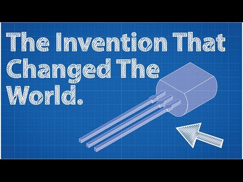 Photo: N43 and Hermes
The transistor emerged from a long chain of materials research, imperfect experiments, institutional bets, and competing inventions. Its history is less a single eureka than a story about learning to control interfaces.
Video reference: Transistors - The Invention That Changed The World — Real Engineering. Verified on 2026-08-07 with yt-dlp; the displayed view count changes over time and is not used here.
01Before the transistor, a problem of scale
Early electronic systems relied heavily on vacuum tubes. Tubes could amplify and switch, but they were bulky, fragile, power-hungry, and slow to start. Telephone networks and early computers needed a more durable way to control signals. The search for a solid-state alternative was therefore driven by infrastructure as much as by laboratory curiosity.
Crystal detectors had already shown that certain minerals could rectify radio signals. The missing step was a reliable device that could provide controlled gain. That required understanding how impurities, surfaces, and electric fields shape charge inside a solid.
02The junction was the intellectual doorway
By the 1930s and 1940s, semiconductor physics had developed enough to make p-n junctions intelligible. Researchers could describe how carriers move, how depletion regions form, and how a material’s conductivity changes with impurities. These ideas supplied the language for a solid-state amplifier even before the final device geometry was known.
The crucial insight was that surfaces matter. A theoretical field effect could be weakened by electronic states trapped at a semiconductor surface. Solving that practical problem required not just equations but cleaner materials, better contacts, and experimental patience.
03Bell Labs makes a breakthrough
In December 1947, John Bardeen and Walter Brattain demonstrated a point-contact transistor at Bell Telephone Laboratories, with William Shockley leading the broader solid-state program. Their device used contacts placed close together on a semiconductor surface. A small input disturbance altered the current through the material and produced amplification.
The first demonstration was ingenious and temperamental. It did not look like a modern chip transistor, and it was difficult to manufacture consistently. But it established the principle that a solid could provide amplification without a heated cathode or evacuated envelope.
04Two transistor paths, not one
The point-contact device was soon joined by the junction transistor, developed through Shockley’s work and announced in 1948. A junction transistor used carefully arranged semiconductor regions rather than two delicate surface contacts. It was more compatible with a program of reproducible manufacturing and became foundational for discrete electronics.
Later, the field-effect transistor returned to the problem of controlling a channel with an electric field. The metal-oxide-semiconductor structure, demonstrated in practical form in the 1950s, eventually became the dominant building block for dense integrated circuits. History therefore did not move in a straight line from the first transistor to today’s MOSFET; several device ideas matured at different speeds.
05The invention becomes manufacturable
A laboratory demonstration is not an industry. Transistors became transformative only when engineers learned to grow purer crystals, form controlled doped regions, make stable contacts, protect surfaces, and produce devices in batches. Planar processing and photolithography provided a route to making many aligned structures on one wafer.
In 1958 and 1959, Jack Kilby and Robert Noyce independently showed how multiple electronic components could be integrated into a single solid-state circuit. The integrated circuit changed the unit of progress from the individual transistor to the repeatable process that makes millions of them together.
06From laboratories to a global supply chain
The transistor’s later history is also a history of institutions. Universities supplied physics, corporate laboratories supplied long-horizon research, government procurement created early markets, and specialized manufacturers refined process control. Equipment makers, chemical suppliers, designers, and software developers became part of the same expanding ecosystem.
This distributed history matters because no single inventor explains the modern semiconductor. The device depended on a network of people and capabilities that could preserve small gains, share techniques, and turn fragile prototypes into reliable commodities.
The industry’s defining pattern has been more controllable switches per unit area, purchased with extraordinary process complexity.
07The hidden continuity
The most important continuity is methodological. Researchers learned to treat surfaces, defects, interfaces, and variation as first-class engineering objects. Each generation of transistor technology inherited a richer set of measurement tools and process recipes. The result was cumulative progress: not one miracle, but a platform on which the next improvement could stand.
The transistor’s hidden history is therefore a lesson in infrastructure. Breakthroughs become world-changing when institutions can reproduce them, lower their cost, and connect them to other breakthroughs.
A transistor does not create energy: it uses a control voltage to regulate a separate current path.
By N43 and Hermes for Sailor Bob News.


