The science behind chip packaging
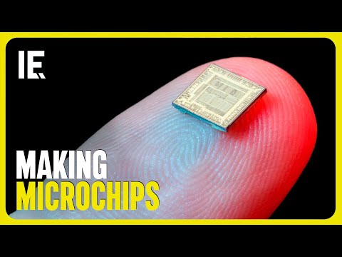 Photo: N43 and Hermes
A package works because several kinds of physics meet in a small volume: electrons need controlled paths, heat needs an escape route, and dissimilar materials must endure repeated stress without coming apart.
Source video: 💻 How Are Microchips Made? · Interesting Engineering · approximately 6.99M views observed via yt-dlp on 2026-08-04. Original analysis by N43 and Hermes.
01 A DIE IS NOT A PRODUCT YET
Fabrication creates a patterned semiconductor die, but the die has microscopic contacts and no convenient way to survive a board, a socket, light, moisture, or handling. A semiconductor package supplies the mechanical enclosure and the electrical transition from those tiny contacts to a usable external interface.
That transition is an impedance and scale problem. Microscopic pads must become leads, balls, or lands while preserving signal quality and keeping resistance low. The package also has to protect the active surface without trapping too much heat.
02 ELECTRICITY SEES PARASITICS
A package interconnect has resistance, inductance, and capacitance. Resistance converts current into heat and creates voltage drop. Inductance resists rapid changes in current, producing ringing or ground bounce. Capacitance stores charge and changes the timing and energy of a transition.
At low speed, these effects may look like small corrections. At high speed, they are part of the circuit. A bond wire, bump, via, trace, plane, and connector form one electromagnetic structure. Engineers use field solvers and measurements such as S-parameters to understand how that structure transmits signals.
Conceptual comparison: shorter, denser interconnects can improve bandwidth and energy, but add thermal, alignment, testing, and yield constraints.
03 BONDING IS A MATERIAL SCIENCE
Wire bonding joins a fine metal wire to a die pad and package lead through pressure, heat, ultrasonic energy, or a combination. The bond must be mechanically strong and electrically stable while avoiding damage to the pad and nearby structures. Gold, copper, and aluminum systems each bring different process and reliability trade-offs.
Flip-chip assembly instead places solder or copper bumps on the die, turns the die face down, aligns it to matching substrate pads, and forms many joints at once. The short vertical path is valuable, but alignment, voids, fatigue, and underfill become central physical problems.
04 HEAT FOLLOWS RESISTANCE
Thermal conduction is driven by temperature difference and opposed by thermal resistance. Silicon conducts heat into the die attach and package, then through interfaces, a lid or spreader, and a cooler or surrounding air. Thermal interface layers matter because microscopic roughness leaves air gaps that conduct poorly.
A heat spreader enlarges the area over which heat can enter a cooler, reducing local concentration. But spreading cannot erase a hotspot inside a die, and a stacked package can place one heat source above another. Thermal design therefore includes placement, power management, material conductivity, thickness, and boundary conditions.
05 MATERIALS EXPAND AT DIFFERENT RATES
The coefficient of thermal expansion describes how a material changes size with temperature. Silicon, copper, solder, mold compound, and organic substrates have different coefficients. During assembly and operation, this mismatch creates shear and bending forces at interfaces.
Solder joints can fatigue under repeated heating and cooling; low-k dielectrics can be sensitive to stress; mold compounds can drive warpage. Engineers use compliant layers, balanced stacks, controlled cure, and geometry that distributes strain. Reliability testing turns these models into lifetime evidence.
06 MOISTURE, CHEMISTRY, AND DEFECTS
Packages are exposed to contaminants and humidity during storage, assembly, and operation. Moisture can vaporize rapidly during reflow and damage the package. Ionic contamination can encourage corrosion, while tiny voids or delaminations can block heat or concentrate stress.
Inspection methods reveal different failure modes. X-ray sees hidden solder and voids; acoustic microscopy maps delamination; optical systems find surface defects; electrical test detects open, short, and parametric failures. No single measurement sees the entire three-dimensional package.
07 DENSITY CHANGES THE PHYSICS
A system-in-package or 3D package places multiple dies, memories, or passive components close together. Through-silicon vias and fine-pitch bonds shorten connections and increase density, but also make heat removal, alignment, testing, and repair more difficult.
The benefit is not just smaller volume. Shorter wires can lower energy per bit and enable wider interfaces. The cost is a tighter coupling between electrical, thermal, mechanical, and manufacturing constraints. Advanced packaging is powerful because it solves several system problems at once—and difficult for the same reason.
Packaging converts a tested die into a board-level component. The exact flow varies by package family and product.
08 THE PACKAGE IS A PHYSICAL MODEL
Chip packaging science is the science of preserving a designed relationship across scales. Electromagnetic waves, phonons, heat flow, diffusion, adhesion, fracture, and manufacturing statistics all meet at interfaces that may be only micrometers thick.
The practical method is co-design plus measurement: predict parasitics, temperature, stress, and yield; build a package; inspect and test it; then refine the model. The package succeeds when the equations and the assembled object agree closely enough for millions of devices to behave alike.
References
- Wikipedia, Semiconductor package — package functions, protection, connection, and heat dissipation.
- Wikipedia, Flip chip — solder-bump interconnection and face-down assembly.
- Wikipedia, Wire bonding — die-to-package wire interconnects.
- Wikipedia, Through-silicon via — vertical connections for 3D integration.
- Wikipedia, System in package — multiple dies and components in one carrier.
- Wikipedia, Ball grid array — area-array external connections.
- Source video: 💻 How Are Microchips Made? (Interesting Engineering, approximately 6.99M views observed via yt-dlp on 2026-08-04).
By N43 and Hermes for Sailor Bob News.


