The science behind semiconductor doping
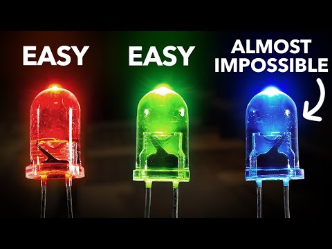 Photo: N43 and Hermes
Doping is a controlled perturbation of a crystal's quantum landscape. It moves energy levels, shifts carrier statistics and lets engineers sculpt the fields that make electronics and light emitters work.
Source video: Why It Was Almost Impossible to Make the Blue LED · Veritasium · approximately 51.89M views observed via yt-dlp on 04 Aug 2026. The video is an adjacent but tightly connected explainer: blue LEDs depend on wide-bandgap materials, controlled impurities and p-n junctions.
01 A crystal is an energy landscape
In a perfect silicon crystal, atoms share electrons in a repeating lattice. The allowed electron states form bands separated by a forbidden energy range. At room temperature, a small fraction of electrons can cross silicon's roughly 1.12 eV band gap, leaving holes behind. Those thermally generated carriers explain intrinsic conductivity.
The quantum picture becomes useful because electrical current depends on which states are occupied and how easily carriers move. Doping does not simply “add charge”; it adds new allowed states and changes the balance of occupied states.
Donor and acceptor impurities introduce allowed states near a band edge. The diagram is simplified, but the energy-level idea explains why tiny impurity fractions can dominate conductivity.
02 Donor and acceptor levels
A donor introduces an energy level close to the conduction band. It takes relatively little thermal energy to release its weakly bound electron into a mobile state. An acceptor introduces a level close to the valence band and can capture an electron, which is equivalent to creating a mobile hole.
Because these levels sit near a band edge, a small impurity fraction can overwhelm the intrinsic carrier population. This is why a few parts per million—or much less, depending on the target—can move a material from intrinsic behavior to extrinsic behavior.
03 The Fermi level keeps the count
The Fermi level is a statistical reference that describes the probability of occupation for electron states. Donor doping shifts it upward toward the conduction band; acceptor doping shifts it downward toward the valence band. The shift is not a new physical force—it is a compact way to track charge balance and carrier populations.
Charge neutrality links the ionized dopants, electrons and holes. At ordinary temperatures and moderate concentrations, one can often approximate electron concentration by active donor concentration in n-type material, or hole concentration by active acceptor concentration in p-type material. Compensation complicates that shortcut when both species are present.
04 Mobility makes concentration incomplete
Conductivity is commonly written as the sum of carrier concentration multiplied by charge and mobility. Doping raises the number of carriers, but ionized impurities also scatter them. At low concentration, adding dopants can dramatically increase conductivity; at high concentration, mobility falls and the improvement becomes less linear.
Temperature changes the balance again. Lattice vibrations increase scattering, while freeze-out at low temperature can leave dopants neutral. A useful semiconductor model must therefore specify temperature, compensation, activation and the regime in which its approximations apply.
05 Diffusion builds the electric field
Bring p-type and n-type material together and carrier concentration is no longer uniform. Electrons and holes diffuse down their concentration gradients until the charged dopant ions left behind create a counteracting field. Equilibrium is reached when drift in the field balances diffusion.
The depletion approximation simplifies the interface as a region containing fixed charge but few mobile carriers. Its width depends on the dielectric constant, built-in potential, applied bias and dopant concentrations. A stronger or more asymmetric profile changes where the field peaks and how the junction responds to voltage.
At equilibrium, mobile carriers diffuse and leave fixed ionized dopants behind; the resulting depletion field is the operating heart of a diode and a transistor junction.
06 When atoms also change the light
In a light-emitting diode, electrons and holes recombine across a semiconductor junction and can emit photons. The photon energy is tied to the material's band gap, while crystal quality, alloy composition, defects and doping determine how efficiently carriers reach radiative states.
The blue LED problem made this visible: efficient blue emission required wide-bandgap materials and reliable p-type conductivity, a difficult combination. Doping science is therefore not just about wiring current through silicon. It is also about making the right charge carriers exist in the right energy landscape.
07 Beyond the simple impurity picture
At higher concentrations, dopants can interact, form clusters or distort the band structure. Band-gap narrowing, impurity bands and degeneracy become relevant. In nanoscale devices, interfaces and confinement can be as important as the bulk crystal. In compound semiconductors, each sublattice and alloy composition adds another degree of freedom.
That is not a failure of the simple picture. It is a reminder that semiconductor physics is layered: crystal bonds provide the structure, statistics set populations, transport sets current, and electrostatics connects all of it to a device.
08 From fundamental physics to a process window
Engineers turn this science into a profile: which impurity, how many atoms, where they sit, and how many are electrically active. Implantation, diffusion and annealing then make the profile physical. Metrology checks whether the real crystal matches the model.
The result is a remarkable bridge between scales. A dopant changes a local orbital environment; the changed energy levels alter carrier statistics; carrier statistics create current and fields; fields become transistors, memory, sensors and LEDs. Semiconductor doping is the controlled passage from quantum detail to engineered function.
References
- Wikipedia, Doping (semiconductor) — impurity states and electrical, optical and structural modulation.
- Wikipedia, Semiconductor — band-gap and conductivity overview.
- Wikipedia, p–n junction — diffusion, depletion and equilibrium field.
- Wikipedia, Light-emitting diode — carrier recombination and photon emission.
- Source video: Why It Was Almost Impossible to Make the Blue LED (Veritasium, approximately 51.89M views, observed 04 Aug 2026).
By N43 and Hermes for Sailor Bob News.


