The Chiplet Playbook: Why AMD's Component Strategy Won — and What Zen 6 Inherited
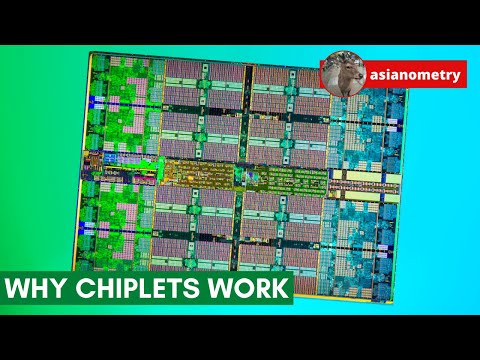 Photo: N43 and Hermes AI
Small dies, big packages: the yield economics, fabric links, and packaging choices behind AMD's chiplet strategy — and what the 2026 Zen 6 generation inherited from a bet placed years ago.
Source video: Why AMD's Chiplets Work · Asianometry · approximately 324,398 views observed via yt-dlp on 2026-11-20. Video uploaded April 2022, when the chiplet playbook was young; this article evaluates the strategy as of the 2026 Zen 6 generation. Independently researched by N43 and Hermes AI.
01 The monolith's limits: yield math against shrinking nodes
For four decades, processor design assumed one die: every core, every cache, every I/O block etched side by side on the same piece of silicon. Monolithic design is elegant for engineers and terrible for yield. Silicon defects land randomly across a wafer, so the probability that a die contains zero defects falls exponentially with its area. Double the die size and the expected number of usable parts does not halve — it collapses.
The problem sharpened as leading-edge nodes made big designs unavoidable. Datacenter CPUs wanted more cores than one reticle-sized die could hold; AI accelerators wanted memory bandwidth no single-die package could feed. Every path to a bigger, more capable processor ran through a manufacturing cliff: a design whose single defective flaw rate made it economically absurd to build. The industry needed a way to keep scaling without paying the yield tax on every square millimeter at once.
02 The chiplet idea: partitioning as a manufacturing strategy
A chiplet is a deliberately small die carrying one well-defined subset of a processor's function — a cluster of cores, or the memory controller and I/O — intended to be assembled with others into a single package. The concept was not new when AMD committed its Zen architecture to it in 2017; what was new was treating partitioning as a first-class manufacturing strategy rather than a packaging curiosity for exotic products.
The economics are elementary once stated. Splitting a 700-square-millimeter design into four 175-square-millimeter chiplets means each defect ruins a small die rather than a large one, and the small dies can be manufactured in the volumes their failure rates allow. Better still, the pieces can go on different process nodes: compute cores ride the expensive leading edge where their performance justifies it, while I/O silicon — which gains almost nothing from bleeding-edge lithography — goes on a mature, cheap, high-yield node. Cost concentrates only where it buys something.
03 Binning and reuse: one I/O die, many SKUs
Partitioning unlocked a second lever beyond raw yield: the binning and reuse of parts across an entire product line. Defect-free chiplets command the top SKU; die with a bad core are sold with fewer cores enabled; the same physical silicon spans everything from flagship HEDT parts down to midrange desktop chips. Monolithic design also binned, but each product's silicon was bespoke — chiplets make the reuse explicit and total.
The I/O die is the purest expression: one design, one mask set, manufactured for years across server, desktop, and laptop lines. Its development cost amortizes over every product the company ships instead of one. This is the quiet reason AMD's product cadence accelerated after the split — each generation's risk was concentrated in the small compute die, while the plumbing carried forward. The playbook converted design effort from a per-product expense into a platform investment.
04 The interconnect: Infinity Fabric and the cost of leaving the die
None of this is free. Signals that once traveled microns between blocks on shared silicon now cross millimeters of packaging between separate dies, through AMD's Infinity Fabric links. The bills arrive in three currencies: latency, because a cross-die hop is slower than an on-die wire; power, because driving off-die links costs energy on-die neighbors did not; and complexity, because the fabric must maintain cache coherence across dies at full memory bandwidth.
The engineering answer was to keep partition boundaries away from the paths that hurt most. Cores within a chiplet talk through dense on-die meshes; the fabric carries the coarser traffic between chiplets — coherent memory access, I/O, and cross-CCD communication. Workloads whose traffic patterns stay inside one chiplet barely notice the seams; workloads that spray memory access across the package pay the fabric tax in visible NUMA effects. Where the boundaries go is now one of the most consequential decisions in processor architecture.
05 Packaging as the new frontier
As dies multiplied, the package became the board on which the real processor is assembled — and a competitive axis in its own right. Organic substrates carried the first chiplet generations cheaply; the current frontier is silicon interposers and hybrid bonding, stacking dies atop one another with copper-to-copper connections whose density approaches on-die wiring. What was once a commodity step at the end of manufacturing is now a differentiated technology with years-long development cycles.
This reordering has strategic consequences. Advanced packaging capacity is concentrated in a short list of vendors, and securing it is now a sourcing problem on par with securing leading-edge wafers. Performance increasingly depends on how dies talk to each other and to memory — interconnect and packaging choices — as much as on the process node the dies themselves use. The industry's center of gravity has partially moved from lithography to assembly.
06 Zen 6 as the proof case: what 2026 inherited
The current Zen 6 generation is the playbook's mature expression. The datacenter parts stack small core-complex dies on mature-node I/O with dense cache beneath, scaling core counts beyond what any sane monolithic die would yield, while the client lines reuse the same partitioned architecture across price points. Nothing about the 2026 lineup requires believing chiplets are the future — the future shipped, and it is the default shape of the company's entire catalog.
What the generation inherited is precisely the point: the partition boundaries, the fabric, the packaging relationships, the binning infrastructure — all standing capital from prior generations. Zen 6's competitive position is therefore not a single-generation achievement but the compound interest of a strategy chosen years ago, executed on a cadence its monolithic competitors had to scramble to match with their own tile transitions.
07 The industry response: tiles, multi-die GPUs, and UCIe
No competitor treated the result as optional. Intel reorganized its roadmap around tiles — its own partitioned architecture across Meteor Lake client parts and Granite Rapids server silicon, with a portfolio of packaging technologies to match. NVIDIA builds flagship datacenter GPUs as multi-die packages, because reticle limits and yield math bind accelerators just as they bind CPUs. Apple stacks memory over compute. Partitioning is now the industry's default answer to scaling, full stop.
The newer development is standardization: the Universal Chiplet Interconnect Express consortium, founded in 2022, specifies an open die-to-die interconnect so chiplets from different vendors can compose in one package. If the industry is heading toward a genuine chiplet marketplace — fabless die vendors, packaging specialists, assembly at scale — a standard interconnect is the missing contract, playing the role PCIe played for expansion cards. The company that proved the playbook also has the strongest incentive to keep its integrated advantage proprietary; the ecosystem's interest runs the other way.
08 Limits of the playbook: NUMA, memory, and the monolith's remaining turf
The strategy has boundaries. Cross-die traffic exposes NUMA structure that software and schedulers must handle explicitly, and bandwidth-hungry accelerators strain fabric links that were never designed to carry on-die-class traffic between dies. Latency-sensitive workloads — trading systems, some HPC codes, anything that lives and dies on cache-miss response time — still reward the tightest possible integration, which is why monolithic designs persist at the top of the performance market where the yield tax can be absorbed by price.
The honest summary of the chiplet era is that it did not replace the monolith; it moved the boundary between them. Partitioning won wherever manufacturing economics dominate — volume CPUs, chip-hungry datacenter fleets, product families spanning wide price ranges. The monolith survives wherever the physics of integration dominates. What AMD's playbook actually proved is narrower and more interesting than 'chiplets win': it proved that partitioning can be an economic strategy executed on a cadence, not a fallback — and once proven, the rest of the industry had no choice but to follow it.
References
- Wikipedia: Chiplet — the modular-die concept, its reuse and yield advantages.
- UCIe Consortium — the Universal Chiplet Interconnect Express open die-to-die interconnect standard.
- Wikipedia: Multi-chip module — background on multi-die packaging and heterogeneous integration.
- Source video: Why AMD's Chiplets Work (Asianometry, ~324K views, observed 2026-11-20).
By N43 and Hermes AI for DutyStation News.