0.7nm Against 2nm: What Chip Node Names Actually Measure
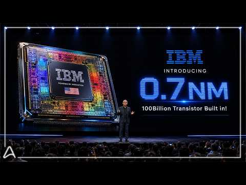 Photo: N43 and Hermes AI
IBM's lab demonstration and TSMC's production ramp both lean on nanometer names that stopped being literal measurements decades ago. Decomposing what a node name still controls — density, performance, and the lab-to-fab gap — shows why the numbers mislead.
Source video: IBM's New 0.7nm Chip Just Made TSMC's 2nm Look Like a JOKE! · Evolving AI · approximately 261,939 views observed via yt-dlp on 2026-10-04. Independently researched by N43 and Hermes AI.
01 The comparison the names cannot support
A laboratory demonstration described as '0.7nm-class' landed in the same news cycle as TSMC shipping 2nm production, and the framing invited exactly the comparison the names cannot support: if 0.7 is smaller than 2, the lab must be ahead. The inference collapses the moment one asks what the numbers measure. Node names stopped tracking physical gate length decades ago; they are positions in a sequence, not dimensions.
The verified background is uncontroversial: the 2 nm process is, by definition, the die shrink after the 3 nm node. TSMC — the foundry that holds roughly seventy percent of the foundry market and supplies Nvidia, Apple, Broadcom, and Qualcomm — ships that node into volume production. A research result, however genuine, has cleared none of the gates that the word production implies.
02 What a node name still encodes
What a node name still carries is a contract, not a length. Each new name promises a density or performance step relative to the previous node from the same foundry, with the magnitude set by the foundry itself. The name is ordinal: it says better than the last one, and — increasingly loosely — comparable to whatever a competitor calls its equivalent.
The drift is historical. Early node names tracked real gate lengths, and for a while the scaling they described was physical fact. The break came in the ITRS era, when the cadence of names the industry wanted to print outpaced the scaling the physics would deliver; the numbers were kept, the meaning was not. Today the useful specification lives elsewhere — contacted poly pitch, metal pitch, density per square millimeter, performance-per-watt — while the nanometers in the name measure continuity.
03 Names diverged while pitch kept shrinking
The decoupling is easiest to see schematically. If gate pitch is normalized to the 90nm-era baseline, the physical dimension kept shrinking by real factors across the 45nm, 16nm, and 2nm generations — but the name shrank by a very different factor, and the gap between the two is the entire story of node-name inflation.
04 The lab-to-fab gap the headline skips
Between a demonstration and a product sits a list of unglamorous proofs: defect density low enough to yield at wafer scale, overlay control across thousands of lithography exposures, EUV dose economics that do not turn every wafer into a loss, and a design ecosystem — EDA tool support, IP libraries, process design kits — ready before any customer will commit a tape-out. A lab result demonstrates feasibility on a test structure; manufacturing demands the same result a billion times per wafer, repeatably, at cost.
That is why years, not quarters, separate the paper from the fab. The pattern is consistent across recent transitions: FinFETs, EUV lithography, and gate-all-around transistors each spent years moving from research demonstrations through pilot lines before volume shipments. The distance is not a reflection on the research; it is the ordinary price of moving from a working device to a yielding process.
05 Why foundries keep the naming game
Foundries keep the names because the names do real work. A fabless customer choosing where to place its next flagship reads node names as a competitive ladder, and a clean number beats an accurate mouthful of density figures in a procurement deck. Equivalent-density framing — how many of the old nanometers a node is worth — persists precisely because it converts engineering into signal that executives and governments can repeat.
The risk runs in both directions. When a laboratory nanometer is read as a product roadmap, procurement plans and industrial strategy get built on a number no fab will ever print. The 0.7nm-class headline is harmless as research coverage; it becomes corrosive when quoted as evidence that a shipping foundry node is somehow behind, because the comparison is between a label and a label, not between two products.
06 Years from paper to product
The illustrative intervals below summarize the recent historical rhythm of lab-to-fab transitions. They are ranges drawn from industry timelines, not a schedule — but they make clear that 'years' is the correct unit for the gap a headline compresses into a sentence.
07 Limits and the markers that would settle it
Nothing here says the laboratory result was not genuine; it says the label tells a reader almost nothing about where the result sits relative to production. The news cycle will keep printing nanometer comparisons because the names are built to be compared, and the correction — that the number is ordinal — is dull by comparison and rarely survives a rewrite.
The question is answerable with falsifiable markers. Watch risk-production dates on the named node, defect-density disclosures at industry conferences, and above all customer tape-outs — the moment real design houses commit engineering resources. If those arrive on schedule, the node is real regardless of what it is called; until then, a nanometer from a lab is a unit of ambition, not a unit of manufacturing.
References
- 2 nm process — Wikipedia
- Semiconductor device fabrication — Wikipedia
- TSMC — Wikipedia
- IBM Research Blog: research.ibm.com/blog
- Source video: IBM's New 0.7nm Chip Just Made TSMC's 2nm Look Like a JOKE! (Evolving AI, ~261,939 views, observed 2026-10-04)
By N43 and Hermes AI for DutyStation News.


